by Roberto Piacentini Filho Director, Product Marketing – Design Engineering Software
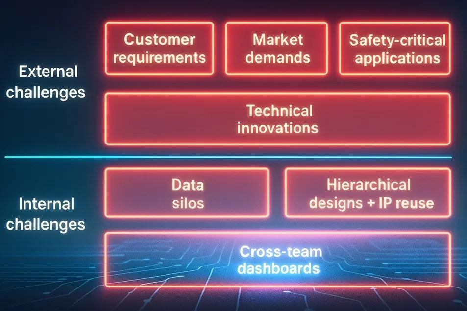
Artificial intelligence is transforming electronic design workflows—but not evenly. While some teams are racing ahead with AI-powered optimization, others remain stuck in the trenches, struggling to find the right version of a file or understand how a reused IP block is behaving in a new context.
The difference isn’t talent. It isn’t budget. It’s data.
Many engineering teams are still battling fragmented design environments. Their data lives across multiple tools, formats, and directories. Version control is inconsistent. Metadata is unreliable. IP reuse is more trial-and-error than strategy. In this kind of chaos, AI-enhanced workflows can’t thrive. They stumble.
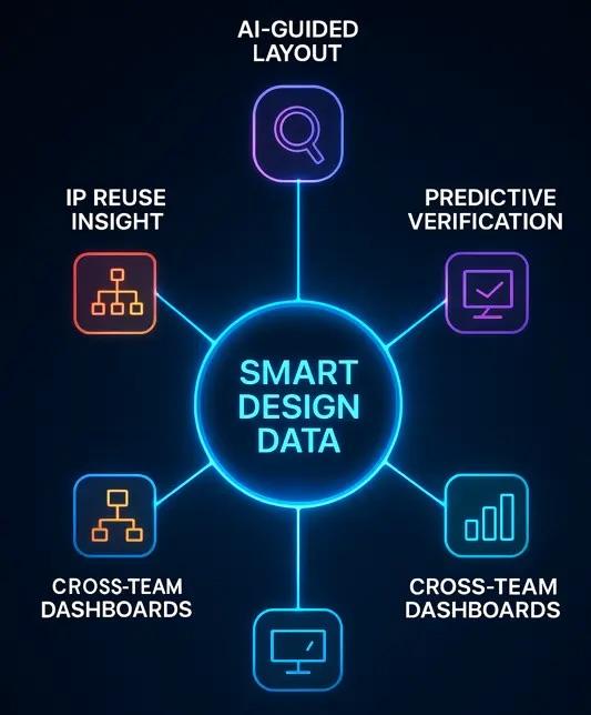
That’s why structured, contextualized, and accessible design data has become the new baseline. It’s not just about getting organized. It’s about unlocking the full potential of the semiconductor development process—from smarter reuse to predictive verification and generative layout.
This article explores what happens when you move beyond cleanup and into capability: how smart design data turns digital exhaust into design intelligence, and how it sets the stage for a new era of competitive advantage.
From Files to Intelligence: The Evolution of Design Data
At many semiconductor companies, "design data" is still treated like a digital filing cabinet. Files are stored, versioned (often manually), and eventually archived. But when data is structured—with contextual metadata, relationship tracking, dependency mapping, and naming standards—it becomes something more: a living, queryable model of your design ecosystem.
This evolution transforms data from a passive artifact into an active source of intelligence. It allows engineers, managers, and even AI models to navigate not just what was built, but how and why it evolved. It introduces history, intent, and trust into every downstream task.
Consider a few practical examples:
- A digital designer looking for a PLL block isn’t browsing folders. They access a curated, filtered list of verified IPs, complete with usage history, test coverage, process compatibility, and performance metrics.
- A layout engineer receives AI-generated constraint recommendations that reflect prior schematic-layout relationships—with embedded awareness of process rules, physical limitations, and historical design tradeoffs.
- A verification engineer opens a failing test case and, with a few clicks, traces it back to the IP version, recent modifications, related regressions, and the teams currently reusing that block elsewhere.
In each case, the intelligence isn’t coming solely from a model. It’s coming from the data. Because the data is clean. Connected. Contextualized.
Five Capabilities Unlocked by Smart Design Data
- Intelligent IP Reuse
The promise of IP reuse is often undermined by uncertainty. Is this IP current? Was it verified? Where else has it been used? Without answers, reuse becomes a liability.
Smart design data answers those questions. It links every IP block to its lineage, test history, project context, and usage footprint. Engineers gain confidence. Reviewers gain traceability. And organizations gain leverage—reducing redundant work, accelerating time-to-market, and embedding knowledge across generations of designs.
- AI-Guided Constraint and Layout Suggestions
AI is only as smart as the examples it learns from. Poorly structured design data yields generic, low-value output. But when historical designs are captured with consistent structure, tagging, and hierarchy, AI can surface real, usable suggestions: constraint blocks, floorplan proposals, routing strategies, and even process-specific optimizations.
This capability transforms layout from a manual bottleneck into a collaborative dialog between engineer and AI. It reduces revision cycles. It preserves design intent. And it scales expertise across teams.
- Predictive Verification and Debug
Verification consumes a massive share of the design timeline—and when it fails, it often fails late. But when test results, coverage metrics, and design changes are linked through structured data, AI can begin to see failure patterns before they fully manifest.
Suddenly, verification isn’t just a pass/fail gate. It’s a feedback loop. Engineers receive early signals. Root causes are identified faster. And post-silicon surprises become far less frequent.
- Faster, Context-Rich Design Reviews
Today, many design reviews still rely on slide decks and screenshots. Discussions are driven by recollection and opinion, not data.
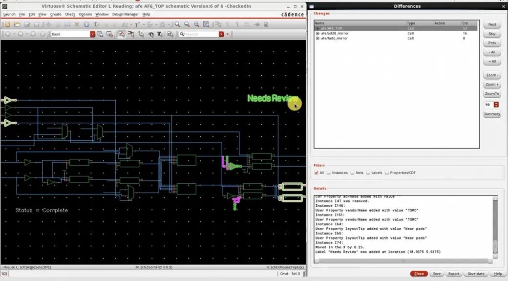
Structured design environments change that. Reviewers can instantly compare revisions, view change propagation across hierarchies, and audit compliance with design standards. Redlines are data-backed. Approvals are traceable. And review cycles become faster, fairer, and more focused.
- Enterprise-Wide Design Intelligence
The benefits of smart data don’t stop with engineering. Product managers want to understand reuse rates and risk exposure. Executives want to benchmark site-to-site performance. Quality teams want traceability for compliance.
When design data is structured and centralized, these questions are no longer painful. They’re answerable. Dashboards become real. Metrics become reliable. And the entire organization becomes more data-informed.
From Friction to Flow: The Human Impact
Engineers often accept daily friction as part of the job. Hunting for the right file. Asking Slack who last touched a design. Revalidating reused blocks. Manually syncing changes across branches. These tasks aren’t innovative. They’re exhausting.
Smart design data eliminates much of this friction. Version history is automatically tracked. Tool outputs are instantly linked to inputs. IP reuse doesn’t require trust—it provides it. The result is flow: engineers staying in focus, staying in tools, and spending more time on innovation and less on archaeology.
Flow doesn’t just improve productivity. It improves satisfaction. It turns reactive workflows into creative ones. And it makes engineering a better experience.
Redefining Integration: More Than APIs
Too often, "EDA integration" means another dropdown menu or export format. But the new generation of design data platforms—like Keysight SOS—redefines integration as embedded intelligence.
These platforms:
- Connect directly with leading design and verification tools
- Interpret data hierarchies, netlists, and metadata in ways software systems cannot
- Synchronize changes across teams, projects, and workflows—in real time
This kind of integration is invisible. Engineers don’t log into it. They work inside it. And when integration works like this, data becomes part of the process—not an afterthought.
Smarter Inputs, Smarter AI
AI doesn’t replace engineers. It amplifies them. But only when it has good inputs. And in the world of chip design, those inputs aren’t just gigabytes—they’re context, history, and structure.
Structured data allows AI to:
- Learn from validated patterns, not just raw files
- Propose edits with awareness of dependencies and constraints
- Deliver insights that are actionable, not abstract
Without structured data, AI becomes generic. With it, AI becomes transformative.
The future of design isn’t fully autonomous. It’s augmented. And smart data is the foundation that makes that augmentation intelligent.
Force-Fit or Purpose-Built? Why the Right Tool Matters
Many semiconductor companies are still trying to retrofit general-purpose software development tools into semiconductor design workflows. Traditional version control systems like Git or other general-purpose version control systems work well for code, but struggle to accommodate the hierarchy, scale, and metadata complexity of chip design. AI compounds this mismatch. Models trained on data designed for software outputs produce brittle or misleading results when applied to silicon.
Force-fitting a dev tool into a design flow creates more problems than it solves. Hierarchies get flattened. Dependencies go untracked. IP reuse becomes opaque. Engineers spend more time working around the tool than with it.
In contrast, purpose-built design data management platforms are optimized for the reality of semiconductor development. They understand IP-centric design. They respect hierarchy. They track relationships across projects and design stages. And, critically, they surface the kind of structured, validated, and contextual data that AI needs to operate reliably.
When you switch from a forced fit to a purpose-built solution, the benefits compound. You not only reduce friction and risk—you unlock new value. AI becomes more accurate, more relevant, and more trusted. Engineering cycles accelerate. Collaboration improves. And your organization moves from struggling to scaling.
Strategic Readiness: Not Just Cleanup—Advantage
It’s tempting to think of data structuring as a hygiene project—important, but invisible. But in reality, structured design data is a strategic differentiator.
It enables faster launches, fewer re-spins, smarter staffing, better collaboration, and ultimately, more innovative products. It empowers leadership with visibility. It empowers engineering with confidence. And it empowers AI with the one thing it truly needs: meaning.
In the era of AI-enhanced EDA, success will not be dictated by who has the flashiest model or the biggest compute cluster. It will be dictated by who has the smartest foundation.
That foundation is design data. Structured. Searchable. Secure. And ready for what’s next.
If your design environment is still fragmented, now is the time to change that. Structure isn’t just about control—it’s the unlock for AI, reuse, speed, and scale. Stop force-fitting yesterday’s tools into today’s challenges.
Build your foundation for tomorrow.
Start organizing. Start optimizing. Start with Keysight SOS.


